You are here
Overview
Application Specific Integrated Circuits are used to design entire systems on a single chip. ASICs are interconnect of standard cells which have been standardized by fabrication houses. With the integration of more and more system components on single IC, the complexity of IC fabrication has increased. Modern day system design involves complex layout issues. Specifications of cells are provided by the vendors in form of Technology library which contains information about geometry, delay and power characteristics of cells.
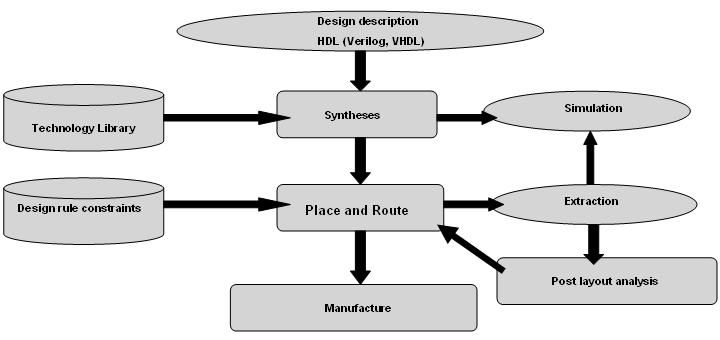
Design flow of ASICs is highly automated. These automation tools provide reasonable performance and cost advantage over manual design process. Broadly ASIC design flow can be divided into following sections :
1. RTL Description: RTL stands for Register Transfer Level. RTL description of a design describes the design in terms registers and logic that resides between them. This captures the timing constraints of the design as well which are nowhere to be seen in behavioral description of the design. Verilog and VHDL are two most popular hardware description languages that are commonly used to write RTL description.
2. Functional Simulation/Verification:Here the RTL description is tested for functional correctness. Simulation involves event and cycle based simulation. While assertion based verification can also be used where formal methods are used to verify the functional correctness of the design.
3. Synthesis: A design description that is functionally correct is fed to a Synthesis tool which extracts Finite State Machine from the design and performs datapath optimizations on the Finite State Machine. The resultant hardware description is mapped to gates, flip-flops and nets to get gate-level netlist. User supplied timing constraints are used to perform timing optimization on gate level netlist.
4. Design Verification: Formal verification methods are used to test the functional correctness of gate-level netlist. Testing functional correctness involves testing an optimized design against a golden design description.
5. Layout: This phase involves floor planning. Placement of cells on the chip area. Placement of Input/Output pads on the chip area. Clock tree synthesis is performed in order to minimize space and power consumed by clock signal. Placement and routing is carried out on this design. So far the interconnect delays and parasitic values are based on wire-load model. Now resistance, capacitance and inductance(latest feature) is calculated for a placed and routed netlist. Design rule violations are identified and corrected. Static timing analysis is carried out to find timing violations.

Figure 1 : ASIC design flow.
