You are here
FPGA Structural Classification
| Programmble Logic Devices
There is a constant effort on the part of system designers to design systems with improved performance, efficiency and flexibility. Today, if one wants to make effective and competitive use of these general purpose blocks, then one of the better ways is to use reconfigurable hardware that allows user programmability. |
The first form of reconfigurable device was Programmable Logic Devices which consisted of arrays of AND and OR gates with programmable metal paths as interconnection between them. They could be programmed to into a single chip to meet specific requirements. PLDs later evolved into what was later known as FPGAs.
Basic structure of an FPGA includes logic elements, programmable interconnects and memory. Arrangement of these blocks is specific to particular manufacturer. On the basis of internal arrangement of blocks FPGAs can be divided into three classes:
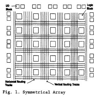
This architecture consists of logic elements(called CLBs) arranged in rows and columns of a matrix and interconnect laid out between them. This symmetical matrix is surrounded by I/O blocks which connect it to outside world. Each CLB consists of n-input Lookup table and a pair of programmable flip flops. I/O blocks also control functions such as tri-state control, output transition speed. Interconnects provide routing path. Direct interconnects between adjacent logic elements have smaller delay compared to general purpose interconnet.

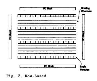
Row based architecture consists of alternating rows of logic modules and programmable interconnect tracks. Input output blocks are located in the periphery of the rows. One row may be connected to adjacent rows via vertical interconnect. Logic modules can be implemented in various combinations. Combinatorial modules contain only combinational elements which Sequential modules contain both combinational elements along with flip flops. This sequential modules can implement complex combinatorial-sequential functions. Routing tracks are divided into smaller segments connected by anti-fuse elements between them.

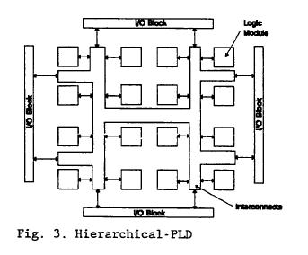
This architecture is designed in hierarchical manner with top level containing only logic blocks and interconnects. Each logic block contains number of logic modules. And each logic module has combinatorial as well as sequential functional elements. Each of these functional elements is controlled by the programmed memory. Communication between logic blocks is achieved by programmable interconnect arrays. Input output blocks surround this scheme of logic blocks and interconnects.

