You are here
Logic Block
Logic BlockLogic block in an FPGA can be implemented in ways that differ in number of inputs and outputs, amount of area consumed, complexity of logic functions that it can implement, total number of transistors that it consumes. This section will describe some important implementations of logic blocks. |
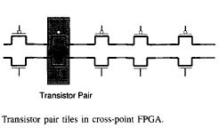
Crosspoint FPGA: consist of two types of logic blocks. One is transistor pair tiles in which transistor pairs run in parallel lines as shown in figure below:

second type of logic blocks are RAM logic which can be used to implement random access memory.
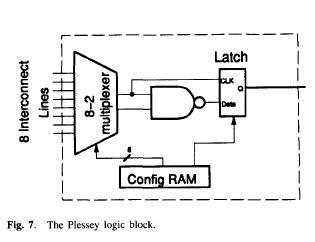
Plessey FPGA: basic building block here is 2-input NAND gate which is connected to each other to implement desired function.

Both Crosspoint and Plessey are fine grain logic blocks. Fine grain logic blocks have an advantage in high percentage usage of logic blocks but they require large number of wire segments and programmable switches which occupy lot of area.
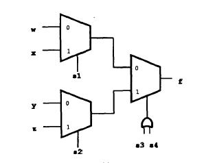
Actel Logic Block: If inputs of a multiplexer are connected to a constant or to a signal, it can be used to implement different logic functions. for example a 2-input multiplexer with inputs a and b, select , will implement function ac + bc´. If b=0 then it will implement ac, and if a=0 it will implement bc´.

Typically an Actel logic block consists of multiple number of multiplexers and logic gates.
Xilinx Logic block:
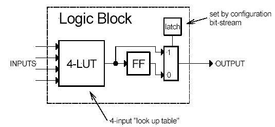
In Xilinx logic block Look up table is used to implement any number of different functionality. The input lines go into the input and enable of lookup table. The output of the lookup table gives the result of the logic function that it implements. Lookup table is implemented using SRAM. A k-input logic function is implemented using 2^k * 1 size SRAM. Number of different possible functions for k input LUT is 2^2^k. Advantage of such an architecture is that it supports implementation of so many logic functions, however the disadvantage is unusually large number of memory cells required to implement such a logic block in case number of inputs is large. Figure below shows 5-input LUT based implementation of logic block.Xilinx - LUT based
LUT based design provides for better logic block utilization. A k-input LUT based logic block can be implemented in number of different ways with tradeoff between performance and logic density.

An n-lut can be shown as a direct implementation of a function truth-table. Each of the latch holds the value of the function corresponding to one input combination. For Example: 2-lut shown in figure below implements 2 input AND and OR functions.

Altera Logic Block
Altera's logic block has evolved from earlier PLDs. It consists of wide fan in (up to 100 input) AND gates feeding into an OR gate with 3-8 inputs. If floating gate transistor based programmable switch is provide any vertical wire passing near AND gate can be used as input to the AND gate. IF each input signal is present both original and complemented form functional capability of block increases significantly. The advantage of large fan in AND gate based implementation is that few logic blocks can implement the entire functionality thereby reducing the amount of area required by interconnects. On the other hand disadvantage is the low density usage of logic blocks in a design that requires fewer input logic.
Another disadvantage is the use of pull up devices (AND gates) that consume static power. To improve power manufacturers provide low power consuming logic blocks at the expense of delay. Such logic blocks have gates with high Threshold as a result they consume less power. Such logic blocks can be used in non-critical paths.
Altera, Xilinx are coarse grain architecture.
Tradeoff - Size of Logic block Vs Performance
Size of logic block plays an important role in deciding density of logic blocks and area utilization in an FPGA. It also effects the performance of the FPGA.
- A large size logic block implements more logic and hence requires less number of logic blocks to implement a functionality on the FPGA. On the other hand a large logic block will consume more space on the FPGA. So optimal size of logic block is one that optimally uses lesser number of logic blocks for functionality implementation while consuming as little space as possible.
- Active logic area is generally less than total logic area due to presence of programmable connections. Total logic area is sum of active logic area and area consumed by programmable connections.
- Routing area in an FPGA is typically more than the active area. It is 70 to 90 percent of total area in an FPGA.
- In case of Lookup table based FPGA, a 4-input lookup table gives best results in terms of logic synthesised and area consumed.
- Granularity of logic block has influence on performance of an FPGA. Typically higher granularity level results in lesser delay between input and output. As the granularity of logic block increases, number of levels of logic in critical path decreases, and hence delay in critical path decreases. On the flip side with increase in granularity level average fan out increases and number of switches also increases as each block has more pins. Also the length of wires increases with increase in size of logic block.
