You are here
FPGA Overview
|
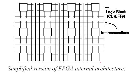
Field Programmable Gate Arrays are two dimensional array of logic blocks and flip-flops with a electrically programmable interconnections between logic blocks. The interconnections consist of electrically programmable switches which is why FPGA differs from Custom ICs, as Custom IC is programmed using integrated circuit fabrication technology to form metal interconnections between logic blocks. |
In an FPGA logic blocks are implemented using mutliple level low fanin gates, which gives it a more compact design compared to an implementation with two-level AND-OR logic. FPGA provides its user a way to configure:
- The intersection between the logic blocks and
- The function of each logic block.
Logic block of an FPGA can be configured in such a way that it can provide functionality as simple as that of transistor or as complex as that of a microprocessor. It can used to implement different combinations of combinational and sequential logic functions. Logic blocks of an FPGA can be implemented by any of the following:
- Transistor pairs
- combinational gates like basic NAND gates or XOR gates
- n-input Lookup tables
- Multiplaexers
- Wide fanin And-OR structure.

Figure 1: Simplefied version of FPGA internal architecture.
Routing in FPGAs consists of wire segments of varying lengths which can be interconnected via electrically programmable switches. Density of logic block used in an FPGA depends on length and number of wire segments used for routing. Number of segments used for interconnection typically is a tradeoff between density of logic blocks used and amount of area used up for routing.
The ability to reconfigure functionality to be implemented on a chip gives a unique advantage to designer who designs his system on an FPGA It reduces the time to market and significantly reduces the cost of production.
Why do we need FPGAs ?
By the early 1980’s Large scale integrated circuits (LSI) formed the back bone of most of the logic circuits in major systems. Microprocessors, bus/IO controllers, system timers etc were implemented using integrated circuit fabrication technology. Random “glue logic” or interconnects were still required to help connect the large integrated circuits in order to :
- generate global control signals (for resets etc.)
- data signals from one subsystem to another sub system.
Systems typically consisted of few large scale integrated components and large number of SSI (small scale integrated circuit) and MSI (medium scale integrated circuit) components.
Intial attempt to solve this problem led to development of Custom ICs which were to replace the large amount of interconnect. This reduced system complexity and manufacturing cost, and improved performance.However, custom ICs have their own disadvantages. They are relatively very expensive to develop, and delay introduced for product to market (time to market) because of increased design time. There are two kinds of costs involved in development of Custom ICs:
1. cost of development and design
2. cost of manufacture
( A tradeoff usually exists between the two costs)
Therefore the custom IC approach was only viable for products with very high volume, and which were not time to market sensitive.
FPGAs were introduced as an alternative to custom ICs for implementing entire system on one chip and to provide flexibility of reporogramability to the user. Introduction of FPGAs resulted in improvement of density relative to discrete SSI/MSI components (within around 10x of custom ICs). Another advantage of FPGAs over CustomICs is that with the help of computer aided design (CAD) tools circuits could be implemented in a short amount of time (no physical layout process, no mask making, no IC manufacturing)
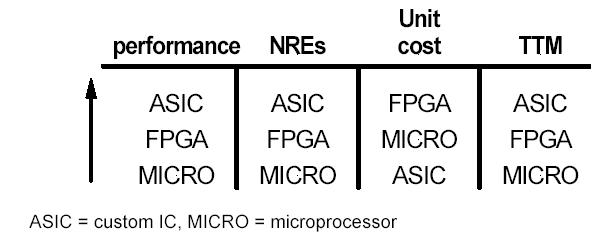
Figure 2: FPGA comparative analysis.
