You are here
FPGA Design Flow
|
One of the most important advantages of FPGA based design is that users can design it using CAD tools provided by design automation companies. Generic design flow of an FPGA includes following steps: |
System Design
At this stage designer has to decide what portion of his functionality has to be implemented on FPGA and how to integrate that functionality with rest of the system.
I/O integration with rest of the system
Input Output streams of the FPGA are integrated with rest of the Printed Circuit Board, which allows the design of the PCB early in design process. FPGA vendors provide extra automation software solutions for I/O design process.
Design Description
Designer describes design functionality either by using schema editors or by using one of the various Hardware Description Languages(HDLs) like Verilog or VHDL.
Synthesis
Once design has been defined CAD tools are used to implement the design on a given FPGA. Synthesis includes generic optimization, slack optimizations, power optimizations followed by placement and routing. Implementation includes Partition, Place and route. The output of design implementation phase is bit-stream file.
Design Verification
Bit stream file is fed to a simulator which simulates the design functionality and reports errors in desired behavior of the design. Timing tools are used to determine maximum clock frequency of the design. Now the design is loading onto the target FPGA device and testing is done in real environment.
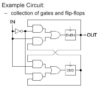
Example :
Below given circuit consists of gates and flip flops. Combinational elements of the circuit are covered by a 4-input Look up table(4-LUT). Sequential elements in the input circuit map to flip flops on the FPGA. Placement of these elements is done in such a way as to minimize wiring during routing.

